Board Support Package For STM32 Microcontroller Boards
Introduction
|
|
|
STM32 F429, F439, F746, F767, H743, H745 Nucleo-144 Boards |

This board support package (BSP) supports STMicroelectronics STM32 F429, F439, F746, F767, H743, H745 boards. The BSP is based on STM32 SDK and uses GNU ARM Embedded compiler tool chain for generating required binaries.
Getting Started
· Install STM32 Nucleo driver from manufacturer website for host PC.
· Create model and build to generate required binary.
· Refer below for programming and debugging support.
Board Configuration
· General Configuration
|
Configuration Parameter |
STM32 Nucleo F429 |
STM32 Nucleo F439 |
STM32 Nucleo F746 |
STM32 Nucleo F767 |
STM32 Nucleo H743 |
STM32 Nucleo H745 |
|
Board Title |
STM32F429 |
STM32F439 |
STM32F746 |
STM32F767 |
STM32H743 |
STM32H745 |
|
Tool Chain Type |
Local Build |
Local Build |
Local Build |
Local Build |
Local Build |
Local Build |
|
Board Preprocessor Symbol |
_BUILD_BRD_STM32F429 |
_BUILD_BRD_STM32F439 |
_BUILD_BRD_STM32F746 |
_BUILD_BRD_STM32F767 |
_BUILD_BRD_STM32H743 |
_BUILD_BRD_STM32H745 |
|
Platform Preprocessor Symbol |
_BUILD_PLT_STM32 |
_BUILD_PLT_STM32 |
_BUILD_PLT_STM32 |
_BUILD_PLT_STM32 |
_BUILD_PLT_STM32 |
_BUILD_PLT_STM32 |
|
Compiler Preprocessor Symbol |
_BUILD_CMP_ARM_GCC |
_BUILD_CMP_ARM_GCC |
_BUILD_CMP_ARM_GCC |
_BUILD_CMP_ARM_GCC |
_BUILD_CMP_ARM_GCC |
_BUILD_CMP_ARM_GCC |
|
C++11 Standard Support |
No |
No |
No |
No |
No |
No |
|
Debug Support |
Yes |
Yes |
Yes |
Yes |
Yes |
Yes |
|
File System Support |
No |
No |
No |
No |
No |
No |
|
OpenMP/OpenCL/CUDA Support |
No/No/No |
No/No/No |
No/No/No |
No/No/No |
No/No/No |
No/No/No |
|
Simulation Panel Support |
No |
No |
No |
No |
No |
No |
· Hardware Configuration
|
Configuration Parameter |
STM32 Nucleo F429 |
STM32 Nucleo F439 |
STM32 Nucleo F746 |
STM32 Nucleo F767 |
STM32 Nucleo H743 |
STM32 Nucleo H745 |
|
Number of CPU cores |
1 |
1 |
1 |
1 |
1 |
2 |
|
Dynamic Memory Support |
Yes |
Yes |
Yes |
Yes |
Yes |
Yes |
|
Prefer Fixed/Floating Point |
Floating Point |
Floating Point |
Floating Point |
Floating Point |
Floating Point |
Floating Point |
|
DI/DO Pins |
PB0_LED1_GPIO[0], PB2_GPIO[1], PB5_GPIO[2], PB6_GPIO[3], PB7_LED2_GPIO[4], PB12_GPIO[5], PB14_LED3_GPIO[6], PD7_GPIO[7], PD10_GPIO[8], PD11_GPIO[9], PE0_GPIO[10], PE1_GPIO[11], PE2_GPIO[12], PE3_GPIO[13], PE4_GPIO[14], PE7_GPIO[15], PE8_GPIO[16], PF0_GPIO[17], PF1_GPIO[18], PF2_GPIO[19], PF6_GPIO[20], PF11_GPIO[21], PF12_GPIO[22], PF13_GPIO[23], PF14_GPIO[24], PF15_GPIO[25], PG0_GPIO[26], PG1_GPIO[27], PG2_GPIO[28], PG3_GPIO[29], PG4_GPIO[30], PG5_GPIO[31], PG10_GPIO[32], PG12_GPIO[33], PG15_GPIO[34], PC13_PBSW_GPIO[35] |
PB0_LED1_GPIO[0], PB2_GPIO[1], PB5_GPIO[2], PB6_GPIO[3], PB7_LED2_GPIO[4], PB12_GPIO[5], PB14_LED3_GPIO[6], PD7_GPIO[7], PD10_GPIO[8], PD11_GPIO[9], PE0_GPIO[10], PE1_GPIO[11], PE2_GPIO[12], PE3_GPIO[13], PE4_GPIO[14], PE7_GPIO[15], PE8_GPIO[16], PF0_GPIO[17], PF1_GPIO[18], PF2_GPIO[19], PF6_GPIO[20], PF11_GPIO[21], PF12_GPIO[22], PF13_GPIO[23], PF14_GPIO[24], PF15_GPIO[25], PG0_GPIO[26], PG1_GPIO[27], PG2_GPIO[28], PG3_GPIO[29], PG4_GPIO[30], PG5_GPIO[31], PG10_GPIO[32], PG12_GPIO[33], PG15_GPIO[34], PC13_PBSW_GPIO[35] |
PB0_LED1_GPIO[0], PB2_GPIO[1], PB5_GPIO[2], PB6_GPIO[3], PB7_LED2_GPIO[4], PB12_GPIO[5], PB14_LED3_GPIO[6], PD7_GPIO[7], PD10_GPIO[8], PD11_GPIO[9], PE0_GPIO[10], PE1_GPIO[11], PE2_GPIO[12], PE3_GPIO[13], PE4_GPIO[14], PE7_GPIO[15], PE8_GPIO[16], PF0_GPIO[17], PF1_GPIO[18], PF2_GPIO[19], PF6_GPIO[20], PF11_GPIO[21], PF12_GPIO[22], PF13_GPIO[23], PF14_GPIO[24], PF15_GPIO[25], PG0_GPIO[26], PG1_GPIO[27], PG2_GPIO[28], PG3_GPIO[29], PG4_GPIO[30], PG5_GPIO[31], PG10_GPIO[32], PG12_GPIO[33], PG15_GPIO[34], PC13_PBSW_GPIO[35] |
PB0_LED1_GPIO[0], PB2_GPIO[1], PB5_GPIO[2], PB6_GPIO[3], PB7_LED2_GPIO[4], PB12_GPIO[5], PB14_LED3_GPIO[6], PD7_GPIO[7], PD10_GPIO[8], PD11_GPIO[9], PE0_GPIO[10], PE1_GPIO[11], PE2_GPIO[12], PE3_GPIO[13], PE4_GPIO[14], PE7_GPIO[15], PE8_GPIO[16], PF0_GPIO[17], PF1_GPIO[18], PF2_GPIO[19], PF6_GPIO[20], PF11_GPIO[21], PF12_GPIO[22], PF13_GPIO[23], PF14_GPIO[24], PF15_GPIO[25], PG0_GPIO[26], PG1_GPIO[27], PG2_GPIO[28], PG3_GPIO[29], PG4_GPIO[30], PG5_GPIO[31], PG10_GPIO[32], PG12_GPIO[33], PG15_GPIO[34], PC13_PBSW_GPIO[35] |
PB0_LED1_GPIO[0], PB2_GPIO[1], PB5_GPIO[2], PB6_GPIO[3], PB7_LED2_GPIO[4], PB12_GPIO[5], PB14_LED3_GPIO[6], PD7_GPIO[7], PD10_GPIO[8], PD11_GPIO[9], PE0_GPIO[10], PE1_GPIO[11], PE2_GPIO[12], PE3_GPIO[13], PE4_GPIO[14], PE7_GPIO[15], PE8_GPIO[16], PF0_GPIO[17], PF1_GPIO[18], PF2_GPIO[19], PF6_GPIO[20], PC2_GPIO[21], PC3_GPIO[22], PA0_GPIO[23], PF14_GPIO[24], PF15_GPIO[25], PG0_GPIO[26], PG1_GPIO[27], PG2_GPIO[28], PG3_GPIO[29], PG4_GPIO[30], PG5_GPIO[31], PG10_GPIO[32], PG12_GPIO[33], PG15_GPIO[34], PC13_PBSW_GPIO[35] |
PB0_LED1_GPIO[0][GPIOB], PB2_GPIO[1][GPIOB], PB5_GPIO[2][GPIOB], PB6_GPIO[3][GPIOB], PB7_GPIO[4][GPIOB], PB8_GPIO[5][GPIOB], PB9_GPIO[6][GPIOB], PB14_LED3_GPIO[7][GPIOB], PB15_GPIO[8][GPIOB], PC6_GPIO[9][GPIOC], PC7_GPIO[10][GPIOC], PC8_GPIO[11][GPIOC], PC9_GPIO[12][GPIOC], PC10_GPIO[13][GPIOC], PC11_GPIO[14][GPIOC], PD3_GPIO[15][GPIOD], PD4_GPIO[16][GPIOD], PD5_GPIO[17][GPIOD], PD6_GPIO[18][GPIOD], PD7_GPIO[19][GPIOD], PE0_GPIO[20][GPIOE], PE1_LED2_GPIO[21][GPIOE], PE2_GPIO[22][GPIOE], PE3_GPIO[23][GPIOE], PE4_GPIO[24][GPIOE], PE10_GPIO[25][GPIOE], PE12_GPIO[26][GPIOE], PE15_GPIO[27][GPIOE], PF15_GPIO[28][GPIOF], PG6_GPIO[29][GPIOG], PG8_GPIO[30][GPIOG], PG9_GPIO[31][GPIOG], PG10_GPIO[32][GPIOG], PG12_GPIO[33][GPIOG], PG14_GPIO[34][GPIOG], PC13_PBSW_GPIO[35][GPIOC] |
|
ADC Default Resolution |
12 |
12 |
12 |
12 |
16 |
16 |
|
ADC Pins |
PA0_ADC[0], PA6_ADC[1], PB1_ADC[2], PC2_ADC[3], PA3_ADC[4], PB0_LED1_ADC[5], PC0_ADC[6], PC3_ADC[7], PF10_ADC[8], PF3_ADC[9], PF4_ADC[10], PF5_ADC[11] |
PA0_ADC[0], PA6_ADC[1], PB1_ADC[2], PC2_ADC[3], PA3_ADC[4], PB0_LED1_ADC[5], PC0_ADC[6], PC3_ADC[7], PF10_ADC[8], PF3_ADC[9], PF4_ADC[10], PF5_ADC[11] |
PA0_ADC[0], PA6_ADC[1], PB1_ADC[2], PC2_ADC[3], PA3_ADC[4], PB0_LED1_ADC[5], PC0_ADC[6], PC3_ADC[7], PF10_ADC[8], PF3_ADC[9], PF4_ADC[10], PF5_ADC[11] |
PA0_ADC[0], PA6_ADC[1], PB1_ADC[2], PC2_ADC[3], PA3_ADC[4], PB0_LED1_ADC[5], PC0_ADC[6], PC3_ADC[7], PF10_ADC[8], PF3_ADC[9], PF4_ADC[10], PF5_ADC[11] |
PF11_ADC[0], PF12_ADC[1], PB0_ADC[2], PA3_ADC[3], PC3_ADC[4], PA6_ADC[5], PB1_ADC[6], PC0_ADC[7], PF5_ADC[8], PF3_ADC[9], PF10_ADC[10], PF4_ADC[11] |
PF11_ADC1_CH2[0][ADC1], PA6_ADC1_CH3[1][ADC1], PC0_ADC1_CH10[2][ADC1], PA0_ADC1_CH16[3][ADC1], PB1_ADC2_CH5[4][ADC2], PF14_ADC2_CH6[5][ADC2], PB0_ADC2_CH9 (LED1)[6][ADC2], PA3_ADC2_CH15[7][ADC2], PC2_ADC3_CH0[8][ADC3], PC3_ADC3_CH1[9][ADC3], PF10_ADC3_CH6[10][ADC3], PF6_ADC3_CH8[11][ADC3] |
|
PWM Default Resolution |
16 |
16 |
16 |
16 |
16 |
16 |
|
PWM Pins |
PE9_PWM[0], PE11_PWM[1], PE13_PWM[2], PE14_PWM[3], PA15_PWM[4], PB10_PWM[5], PB11_PWM[6], PB4_PWM[7], PC7_PWM[8], PC8_PWM[9], PD12_PWM[10], PD13_PWM[11], PD14_PWM[12], PD15_PWM[13], PC6_PWM[14], PC9_PWM[15], PE5_PWM[16], PE6_PWM[17], PB14_LED3_PWM[18], PB15_PWM[19] |
PE9_PWM[0], PE11_PWM[1], PE13_PWM[2], PE14_PWM[3], PA15_PWM[4], PB10_PWM[5], PB11_PWM[6], PB4_PWM[7], PC7_PWM[8], PC8_PWM[9], PD12_PWM[10], PD13_PWM[11], PD14_PWM[12], PD15_PWM[13], PC6_PWM[14], PC9_PWM[15], PE5_PWM[16], PE6_PWM[17], PB14_LED3_PWM[18], PB15_PWM[19] |
PE9_PWM[0], PE11_PWM[1], PE13_PWM[2], PE14_PWM[3], PA15_PWM[4], PB10_PWM[5], PB11_PWM[6], PB4_PWM[7], PC7_PWM[8], PC8_PWM[9], PD12_PWM[10], PD13_PWM[11], PD14_PWM[12], PD15_PWM[13], PC6_PWM[14], PC9_PWM[15], PE5_PWM[16], PE6_PWM[17], PB14_LED3_PWM[18], PB15_PWM[19] |
PE9_PWM[0], PE11_PWM[1], PE13_PWM[2], PE14_PWM[3], PA15_PWM[4], PB10_PWM[5], PB11_PWM[6], PB4_PWM[7], PC7_PWM[8], PC8_PWM[9], PD12_PWM[10], PD13_PWM[11], PD14_PWM[12], PD15_PWM[13], PC6_PWM[14], PC9_PWM[15], PE5_PWM[16], PE6_PWM[17], PB14_LED3_PWM[18], PB15_PWM[19] |
PE9_PWM[0], PE11_PWM[1], PE13_PWM[2], PE14_PWM[3], PA15_PWM[4], PB10_PWM[5], PB11_PWM[6], PB4_PWM[7], PC7_PWM[8], PC8_PWM[9], PD12_PWM[10], PD13_PWM[11], PD14_PWM[12], PD15_PWM[13], PC6_PWM[14], PC9_PWM[15], PE5_PWM[16], PE6_PWM[17], PB14_LED3_PWM[18], PB15_PWM[19] |
PE9_TIM1_CH1[0][TIM1], PE11_TIM1_CH2[1][TIM1], PE13_TIM1_CH3[2][TIM1], PE14_TIM1_CH4[3][TIM1], PB10_TIM2_CH3[4][TIM2], PB11_TIM2_CH4[5][TIM2], PC6_TIM3_CH1[6][TIM3], PC7_TIM3_CH2[7][TIM3], PC8_TIM3_CH3[8][TIM3], PC9_TIM3_CH4[9][TIM3], PD12_TIM4_CH1[10][TIM4], PD13_TIM4_CH2[11][TIM4], PD14_TIM4_CH3[12][TIM4], PD15_TIM4_CH4[13][TIM4], PE5_TIM15_CH1[14][TIM15], PE6_TIM15_CH2[15][TIM15] |
|
DAC Default Resolution |
12 |
12 |
12 |
12 |
12 |
12 |
|
DAC Pins |
PA4_DAC[20], PA5_DAC[21] |
PA4_DAC[20], PA5_DAC[21] |
PA4_DAC[20], PA5_DAC[21] |
PA4_DAC[20], PA5_DAC[21] |
PA4_DAC[20], PA5_DAC[21] |
PA4_DAC[16][DAC1], PA5_DAC[17][DAC1] |
|
UART0 Pins |
Via USB Programmer Port (PD9 (RX), PD8 (TX)) |
Via USB Programmer Port (PD9 (RX), PD8 (TX)) |
Via USB Programmer Port (PD9 (RX), PD8 (TX)) |
Via USB Programmer Port (PD9 (RX), PD8 (TX)) |
Via USB Programmer Port (PD9 (RX), PD8 (TX)) |
Via USB Programmer Port (PD9 (RX), PD8 (TX)) |
|
UART1 Pins |
PD6 (RX), PD5 (TX) |
PD6 (RX), PD5 (TX) |
PD6 (RX), PD5 (TX) |
PD6 (RX), PD5 (TX) |
PD6 (RX), PD5 (TX) |
PD6 (RX), PD5 (TX) |
|
UART2 Pins |
PC10 (RX), PC11 (TX) |
PC10 (RX), PC11 (TX) |
PC10 (RX), PC11 (TX) |
PC10 (RX), PC11 (TX) |
PC10 (RX), PC11 (TX) |
PC10 (RX), PC11 (TX) |
|
UART3 Pins |
PD2 (RX), PC12 (TX) |
PD2 (RX), PC12 (TX) |
PD2 (RX), PC12 (TX) |
PD2 (RX), PC12 (TX) |
PD2 (RX), PC12 (TX) |
PD2 (RX), PC12 (TX) |
|
UART4 Pins |
PE7 (RX), PE8 (TX) |
PE7 (RX), PE8 (TX) |
PE7 (RX), PE8 (TX) |
PE7 (RX), PE8 (TX) |
PE7 (RX), PE8 (TX) |
PE7 (RX), PE8 (TX) |
|
SPI Pins |
PF9 (MOSI), PF8 (MISO), PF7 (CLK) |
PF9 (MOSI), PF8 (MISO), PF7 (CLK) |
PF9 (MOSI), PF8 (MISO), PF7 (CLK) |
PF9 (MOSI), PF8 (MISO), PF7 (CLK) |
PF9 (MOSI), PF8 (MISO), PF7 (CLK) |
PF9 (MOSI), PF8 (MISO), PF7 (CLK) |
|
I2C Pins |
Implemented through Soft I2C. PF0 (SDA), PF1 (SCL) |
Implemented through Soft I2C. PF0 (SDA), PF1 (SCL) |
Implemented through Soft I2C. PF0 (SDA), PF1 (SCL) |
Implemented through Soft I2C. PF0 (SDA), PF1 (SCL) |
Implemented through Soft I2C. PF0 (SDA), PF1 (SCL) |
Implemented through Soft I2C. PB9 (SDA), PB8 (SCL) |
|
Ethernet Support |
Implemented through TargetHw_LwIP block |
Implemented through TargetHw_LwIP block |
Implemented through TargetHw_LwIP block |
Implemented through TargetHw_LwIP block |
Implemented through TargetHw_LwIP block |
Implemented through TargetHw_LwIP block |
STM32H745 Dual Core Usage
The BSP supports dual core feature on STM32H745. Following points shall be noted while creating models for this platform
· User can create a single model for programming both cores. Each block in a user created model can be assigned to one of the cores. This can be done by entering core index (starting from zero) in ‘Execution Thread’ parameter of ‘_Block Execution’ group under block parameters.
· Two blocks from different cores cannot be connected.
· While using hardware IO pins (GPIO, ADC, PWM and DACs) it is recommended to use pins from same pin group within a core. Using pins from same pin group across different cores may cause undesired results. Example using ADC1 CH2 in Core1 and ADC1 CH3 in core Core2 is not recommended. Pin group is given along with pin label and pin internal ID in above table. For example for ADC pin ‘PF11_ADC1_CH2[0][ADC1]’ from above table, PG11_ADC1_CH2 is pin label, 0 is internal pin ID and ADC1 is pin group.
· To exchange data between blocks that are assigned to different cores user may use ‘Shared Memory With HSEM’ block.
· Each core shall be build and programmed separately.
· Options for selecting a particular core and other related options are available through target hardware build options on STM32H745 boards as shown below. Please refer to Project Building & Compiling -> Setup Simulation Parameters in CASP documentation on how to invoke Target Hardware Build Options.
· Basic
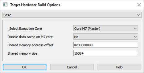
|
Entity Name |
Description |
Default Value |
|
_Select Execution Core |
Select current core to build and program the model |
Core M7 (Master) |
|
Disable data cache on M7 core |
Disables data cache on M7 core. This may be required for some use cases. Proper working of LWIP block requires disabling of data cache on M7 core. |
No |
|
Shared memory address offset |
Enter shared memory address offset |
0x38000000 |
|
Shared memory size |
Enter shared memory allocated size |
16384 |
STM32 Pin out
|
|
|
|


Programmer
CASP supports Programmer0 (using stlink_cli.exe) for uploading generated hex file to the board.
Debugging
Debugging is supported over USB serial.
Known Issues & Limitations
· On STM32H745 ‘TargetHw LWIP’ block is currently having issues when executing on M7 core when data cache in enabled. As a work around disable data cache on M7 core or shift LWIP block to M4 core.