TI C2000 Platform Board Support Package
Introduction
|
|
|
LAUNCHXL-F280049C Board |
|
|
|
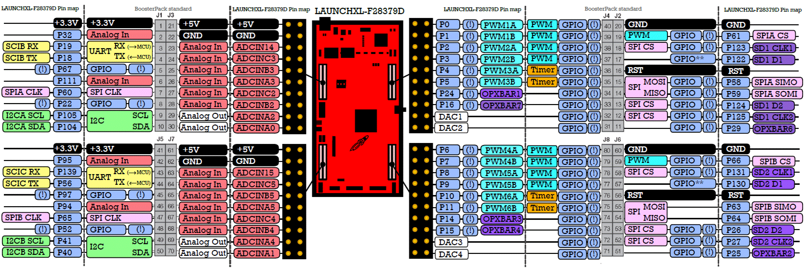
LAUNCHXL-F28379D Board |

This board support package (BSP) supports Texas Instruments (TI) LAUNCHXL-F280049C and LAUNCHXL-F28379D boards.
· This BSP is based on TI’s C2000 compiler tool chain that comes as part of TI Code Composer Studio and uses TI Bit-Field and C2000Ware v3.04.00.00.
· Supports most of the generic peripherals such as GPIOs (with five digital input interrupts), PWM, ADCs, DACs, Serial, SPI and I2C. While communicating with other devices, only even data lengths are supported.
· Supports uploading generated binary to RAM and flash memories.
Getting Started
· Install TI Code Composer Studio along with USB driver software on Windows host system. C2000Ware need not be installed as it is provided as part of CASP BSP.
· Install this CASP TI BSP. Procedure for installation of BSP is explained under Introduction -> Installation section of CASP main documentation.
· Set the C2000 compiler and programmer paths. For this run CASP. Press Start button on top left corner, go to Settings, select the required target hardware board and right click to select Add. Board Variables. A window appears as shown below. Enter the C2000 compiler tool chain bin path under <tc_path> field and debug server paths under <prog0_path> and <prog1_path>. The below figure shows typical paths. Save the settings before closing the window.

· Create model and build to generate required binary.
· Refer below for programming and debugging support.
LAUNCHXL- F280049C Configuration
· General Configuration
|
Configuration Parameter |
Parameter Value |
|
Board Title |
LaunchXL_F280049C |
|
Tool Chain Type |
Local Build |
|
Board Preprocessor Symbol |
_BUILD_BRD_LXL_F280049C |
|
Platform Preprocessor Symbol |
_BUILD_PLT_TI_C28X |
|
Compiler Preprocessor Symbol |
_BUILD_CMP_TI_CL2000 |
|
C++11 Standard Support |
No |
|
Debug Support |
Yes |
|
File System Support |
No |
|
OpenMP/OpenCL/CUDA Support |
No/No/No |
|
Simulation Panel Support |
No |
· Hardware Configuration
|
Configuration Parameter |
Parameter Value |
Remarks |
|
Number of CPU cores |
1 |
|
|
Dynamic Memory Support |
Yes |
|
|
Prefer Fixed/Floating Point |
Floating Point |
|
|
DI/DO Pins |
3[13], 4[40], 7[56], 9[37], 10[35], 11[59], 12 (LED RED)[23], 13[39], 14[17], 15[16], 19[57], 31[25], 32[18], 33[30], 34[58], 35[5], 36[4], 37[9], 38[8], 39[11], 40[10], 47[22], 51[12], 52 (LED GREEN)[34], 53[33], 54[31], 55[24], 59[27], 71[32], 72[14], 73[15], 74[26], 75[3], 76[2], 77[7], 78[6], 79[1], 80[0] |
|
|
ADC Default Resolution |
12 |
|
|
ADC Pins |
8[36], 23[5], 24[16], 25[34], 26[17], 27[18], 28[32], 29[9], 45[20], 46[4], 48[8], 63[6], 64[22], 65[46], 66[33], 67[35], 68[37], 69[3], Internal Temperature[30] |
|
|
PWM Default Resolution |
12 |
|
|
PWM Pins |
35[5], 36[4], 37[9], 38[8], 39[11], 40[10], 71[15], 72[14], 75[3], 76[2], 77[7], 78[6], 79[1], 80[0] |
|
|
DAC Default Resolution |
12 |
|
|
DAC Pins |
30[252], 70[251] |
|
|
UART0 |
Via USB Programmer Port. SCIA of LaunchXL is used for UART0. |
Implemented through TargetHw_Serial block. |
|
UART1 Pins |
SCIB of LaunchXL is used for UART1. Please refer to above figures for corresponding pins. |
Implemented through TargetHw_Serial1 block |
|
SPI and SPI1 Pins |
SPIA and SPIB of LaunchXL are used for SPI and SPI1 respectively. Please refer to above figures for corresponding pins. |
Implemented through SPI and SPI1 interfaces. Refer SPI.h from BSP directory |
|
I2C Pins |
I2CA of LaunchXL is used for I2C. Please refer to above figures for corresponding pins. |
Implemented through I2C interface. Refer Wire.h from BSP directory |
LAUNCHXL- F280049C Usage Considerations
· Buffered DAC has maximum output voltage of 3.3v. User may enable DAC_VREF_FROM_VDAC in c2000.h file to enable external VRef.
· Common timer is used for PWM pin pairs [35,36], [37,38], [39,40], [71,72], [75,76], [77,78], [79,80]. As such if PWM period is changed for one pin other pin period will also changes within same pair.
· Target Hardware Build Options. Please refer to Project Building & Compiling -> Setup Simulation Parameters in CASP documentation on how to invoke Target Hardware Build Options.
· Basic

|
Entity Name |
Description |
Default Value |
|
Program To |
Select program to RAM and FLASH |
RAM |
|
Compiler Debug Switch |
Select enable of disable compiler debug switch --define=DEBUG. |
Disable |
LAUNCHXL- F28379D Configuration
· General Configuration
|
Configuration Parameter |
Parameter Value |
|
Board Title |
LaunchXL_F28379D |
|
Tool Chain Type |
Local Build |
|
Board Preprocessor Symbol |
_BUILD_BRD_LXL_F28379D |
|
Platform Preprocessor Symbol |
_BUILD_PLT_TI_C28X |
|
Compiler Preprocessor Symbol |
_BUILD_CMP_TI_CL2000 |
|
C++11 Standard Support |
No |
|
Debug Support |
Yes |
|
File System Support |
No |
|
OpenMP/OpenCL/CUDA Support |
No/No/No |
|
Simulation Panel Support |
No |
· Hardware Configuration
|
Configuration Parameter |
Parameter Value |
Remarks |
|
Number of CPU cores |
2 |
|
|
Dynamic Memory Support |
Yes |
|
|
Prefer Fixed/Floating Point |
Floating Point |
|
|
DI/DO Pins |
LED (RED)[34], LED (BLUE)[31], 2[32], 3[19], 4[18], 7[60], 9[105], 10[104], 11[29], 12[125], 13[124], 14[59], 15[58], 17[122], 18[123], 19[61], 33[16], 34[24], 35[5], 36[4], 37[3], 38[2], 39[1], 40[0], 42[95], 43[139], 44[56], 47[65], 49[41], 50[40], 51[25], 52[27], 53[26], 54[64], 55[63], 57[130], 58[131], 59[66], 73[15], 74[14], 75[11], 76[10], 77[9], 78[8], 79[7], 80[6] |
|
|
ADC Default Resolution |
12 |
|
|
ADC Pins |
23 (ADCA14)[14][ADCA], 23 (ADCB14)[30][ADCB], 23 (ADCC14)[46][ADCC], 23 (ADCD14)[62][ADCD], 24 (ADCC)[35][ADCC], 25 (ADCB)[19][ADCB], 26 (ADCA)[3][ADCA], 27 (ADCC)[34][ADCC], 28 (ADCB)[18][ADCB], 29 (ADCA)[2][ADCA], 30 (ADCA0)[0][ADCA], 30 (ADCA12)[12][ADCA], 30 (ADCB12)[28][ADCB], 30 (ADCC12)[44][ADCC], 30 (ADCD12)[60][ADCD], 63 (ADCA15)[15][ADCA], 63 (ADCB15)[31][ADCB], 63 (ADCC15)[47][ADCC], 63 (ADCD15)[63][ADCD], 64 (ADCC)[37][ADCC], 65 (ADCB)[21][ADCB], 66 (ADCA)[5][ADCA], 67 (ADCC)[36][ADCC], 68 (ADCB)[20][ADCB], 69 (ADCA)[4][ADCA], 70 (ADCA1)[1][ADCA], Internal Temperature (ADCA)[13][ADCA], 1 (J21 ADCD)[48][ADCD], 3 (J21 ADCD)[49][ADCD], 5 (J21 ADCD)[50][ADCD], 7 (J21 ADCD)[51][ADCD] |
|
|
PWM Default Resolution |
12 |
|
|
PWM Pins |
35 (PWM3)[5][PWM3], 36 (PWM3)[4][PWM3], 37 (PWM2)[3][PWM2], 38 (PWM2)[2][PWM2], 39 (PWM1)[1][PWM1], 40 (PWM1)[0][PWM1], 75 (PWM6)[11][PWM6], 76 (PWM6)[10][PWM6], 77 (PWM5)[9][PWM5], 78 (PWM5)[8][PWM5], 79 (PWM4)[7][PWM4], 80 (PWM4)[6][PWM4] |
|
|
DAC Default Resolution |
12 |
|
|
DAC Pins |
30 (DACA)[251][DACA], 70 (DACB)[252][DACB] |
|
|
UART0 |
Via USB Programmer Port. SCIA of LaunchXL is used for UART0. |
Implemented through TargetHw_Serial block. Configure CPU2 core for SCIA from target build options (given below) if this block is executed on CPU2. |
|
UART1 Pins |
SCIB of LaunchXL is used for UART1. Please refer to above figures for corresponding pins. |
Implemented through TargetHw_Serial1 block. Configure CPU2 core for SCIB from target build options (given below) if this block is executed on CPU2. |
|
SPI Pins |
SPIA and SPIB of LaunchXL are used for SPI and SPI1 respectively. Please refer to above figures for corresponding pins. |
Implemented through SPI and SPI1 interfaces. Refer SPI.h from BSP directory. Configure CPU2 core for SPIA and SPIB from target build options (given below) if this block is executed on CPU2. |
|
I2C Pins |
I2CA of LaunchXL is used for I2C. Please refer to above figures for corresponding pins. |
Implemented through I2C interface. Refer Wire.h from BSP directory. Configure CPU2 core for I2CA from target build options (given below) if this block is executed on CPU2. |
LAUNCHXL- F28379D Usage Considerations
· ADC VRef. is 3.0v.
· Buffered DAC has maximum output voltage of 3.0v.
· Common timer is used for PWM pin pairs [35,36], [37,38], [39,40], [75,76], [77,78], [79,80]. As such if PWM period is changed for one pin other pin period will also changes within same pair.
· The BSP supports dual core feature available on F28379D. Following points shall be noted while creating models for this platform
· User can create a single model for programming both cores. Each block in a user created model can be assigned to one of the cores. This can be done by entering core index (starting from zero) in ‘Execution Thread’ parameter of ‘_Block Execution’ group under block parameters.
· Two blocks from different cores cannot be connected.
· While using hardware IO pins (GPIO, ADC, PWM and DACs) it is recommended to use pins from same pin group within a single core. Using pins from same pin group across different cores may cause undesired results. Example using ADC1 CH2 in Core1 and ADC1 CH3 in core Core2 is not recommended. Pin group is given along with pin label and pin internal ID in above table. For example for ADC pin ‘26 (ADCA)[3][ADCA]’ from above table, 26 (ADCA) is pin label, 3 is internal pin ID and ADCA is pin group.
· To exchange data between blocks that are assigned to different cores user may use ‘Shared Memory With HSEM’ block. This block uses CPU1 CPU2 message RAM for this purpose.
· Each core shall be build and programmed separately. Dual core mode works only when programmed to flash memory. Also, Core1 should always be programmed after Core2.
· Options for selecting a particular core and other related options are available through target hardware build options as shown below. Please refer to Project Building & Compiling -> Setup Simulation Parameters in CASP documentation on how to invoke Target Hardware Build Options.
· Basic

|
Entity Name |
Description |
Default Value |
|
_Select Execution Core |
Select current core to build and program the model. |
Core1 (Single Core Mode) |
|
Program To |
Select program to RAM and FLASH |
RAM |
|
Compiler Debug Switch |
Select enable of disable compiler debug switch --define=DEBUG. |
Disable |
|
CPU1 RW shared memory offset |
Enter CPU1 read write shared memory that is defined in 2837xd_flash_lnk_xxxxx.cmd and 2837xd_ram_lnk_xxxxx.cmd files. |
“CPU1TOCPU2SHM” |
|
CPU2 RW shared memory offset |
Enter CPU2 read write shared memory that is defined in 2837xd_flash_lnk_xxxxx.cmd and 2837xd_ram_lnk_xxxxx.cmd files. |
“CPU2TOCPU1SHM” |
|
Shared memory size |
Enter shared memory allocated size. Maximum 1024. |
1024 |
· Peripheral CPU2 Selection

|
Entity Name |
Description |
Default Value |
|
All |
Select Yes if respective peripheral is executed on CPU2. |
No |
Programmer
CASP supports two programmers for uploading generated binary file. Programmer0 can be used for uploading the binary file to RAM and FLASH memories. Alternately, Programmer1 can also be used to upload code to RAM and FLASH memories. Use Target Hardware build options from Simulation -> Setup Simulation as shown in below figure to select between RAM and FLASH.

Debugging
Debugging via USB virtual serial COM port is supported. To enable serial port debugging set ‘Code Debug Level’ to Level3 from Setup Simulation->Build tab.
Known Issues & Limitations
· CLA is supported only through custom block code.
· Since C2000 architecture byte size is 16-bit. CASP blocks that use pointer conversion between the byte and other 32-bit and 64-bit data types shall be used cautiously. Most of the blocks from Data Routing group fall into this category,
· This BSP is currently work in progress.