Methods for Logic Development in CASP
This example project demonstrates three different methods of developing the same logic on any given platform or target supported by CASP. For this example we have considered Shakti FPGA soft core platform as target. However, any CASP supported target can be used to demonstrate the three methods. Since the target has multiple on-board LEDs, we create a running lights demo that sequentially on and off the LEDs (LED4 to LED7) available on the board. We also try to control the on-off rate of these LEDs with two push buttons available on the FPGA board.
Method 1: Developing logic through modeling
In this method the running light logic is created with a model. This method does not require programming. Portability between different platforms is ensured with this method.
a) Start CASP and create a new project with a workspace file.
b) Create model as shown below
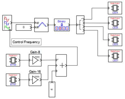
Signal generator block on top left of the model is configured to generate square wave output with external frequency control. Output of the signal generator is given to an up counter which counts from 0 to 3. The output of this block is further given to binary to decimal counter that outputs equivalent decimal value for each input binary value. The output of the block is extended to four digital output blocks configured with LED4 to LED7.
The two digital input blocks are configured/ mapped to BTN0 (push button 0) and BTN1 (push button 1) available on the FPGA board. BTN0 with gain 8 and BTN1 with gain 16 are added along with a constant value 4. The output of the added block is used to control the frequency of signal generator. The default output frequency of signal generator is 4 Hz. When BTN0 is pressed the output frequency is set to 12Hz and with BTN1 the output frequency is set to 20Hz.
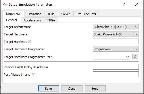
After the model is completed setup the simulation parameters as shown below
1. Set target hardware to Shakti Pinaka with Programmer0
2. Setup simulation runtime settings
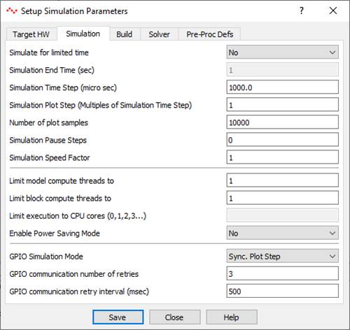
The important setting here is to run the simulation is real time. For this the Simulation Speed Factor shall be set to 1.
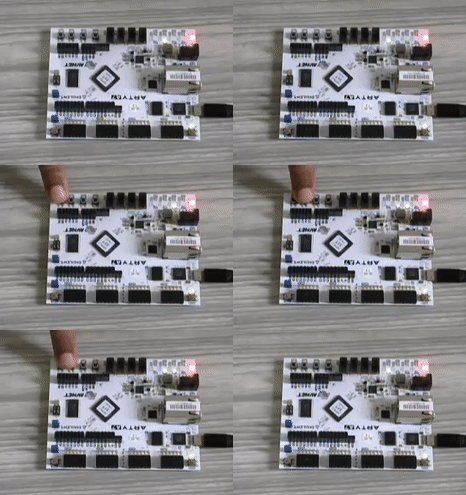
Now connect the FPGA board programmed with Shakti Pinaka MCS file. Ensure USB virtual COM port is assigned with libusbK driver and press Build/Run button on CASP main tool bar. CASP validates and builds the model, compiles the backend generated code and program the FPGA board. The output should look like as shown in below video.
Method 2: Developing logic through custom block
In this method the running light logic is developed in C/C++ within a custom block. A custom block is similar to other blocks in CASP except it is created by the user. User creates a custom block and develops required logic in block’s source file. The developed custom block is then used in the modeling along with other input output blocks to achieve desired output. This method requires programming in C/C++. Since we create a generic logic without dependences on target hardware specific code, this block should be portable between different platforms.
1) Creating Custom Block
Start CASP and click on Tools > Block Editor to open CASP Block Editor. In the Block Editor click on New button and enter block name and version string other block parameters related to block configuration, user parameter configuration, presentation (creating block ports) and block code configuration can be configured. Refer Tutorial-9 on Creating Custom Block for details on how to create CASP blocks. Save the block in the above project directory under /blocks folder by pressing Save button. After configuring required block parameters press ‘Generate Template Code’ under ‘Code’ tab to generate template code. The template code .h and .cpp file will be generated under /bin directory of block folder.
2) Developing Running Light Logic in custom block source file
a) Open generated .h and .cpp in C/C++ editor of your choice. In the header file clean up the unnecessary code and add variables m_prev_time and m_cur_out_idx under private section. The complete code of the header file is shown below
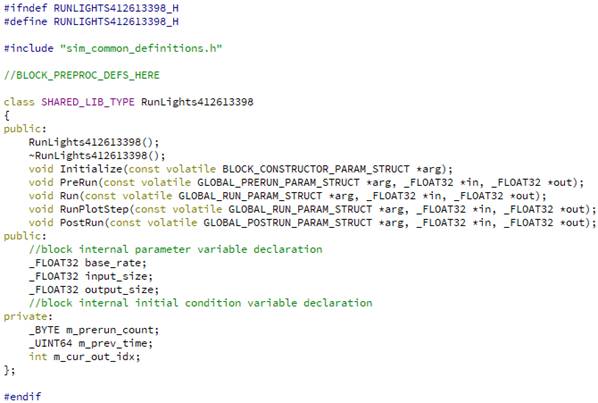
b) Similarly create required logic in Prerun and Run functions in the cpp file. The Prerun function is called during program start up and shall be used to initialize the variables. Run function is called in every time step and shall be used to create actual logic that executes in every step. The complete code of the cpp file is shown below
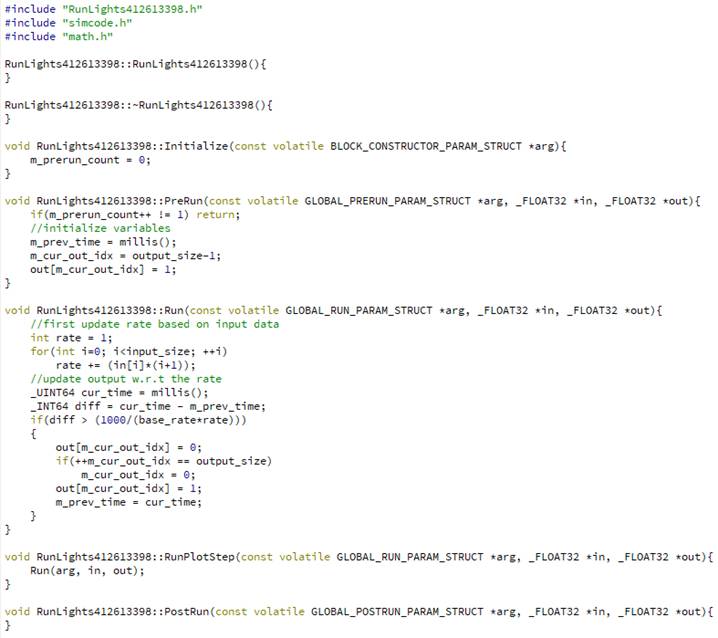
3) Creating required model around the custom block
Insert the custom block we have just created in the existing model and connect input outputs to the block as shown below
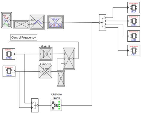
Processing blocks used in Method-1 shall be disabled as these blocks are replaced by the custom block. Set the custom block parameters are shown below
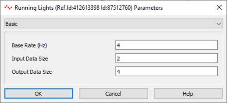
With the same simulation settings of Method-1, press Build/Run button. If errors are present in custom block source code it will be displayed in the Build window. If no errors are present the model will be build and the generated hex file will be uploaded to the FPGA board. The LEDs will start blinking sequentially at a frequency of 4Hz. If BTN0 is pressed the frequency will be doubled and if BTN1 is pressed the frequency will be four times of base frequency.
Method 3: Developing logic through custom block that includes CASP HAL APIs
This method is an extension of Method-2 above. Here CASP HAL APIs are used in custom block code to directly access hardware pins. Since, HAL APIs are specific to hardware BSP, this method is not portable between different platforms. However, this method can be used for debugging and testing. For our running light example the Prerun and Run functions in the .cpp file are modified to use CASP HAL APIs as shown below

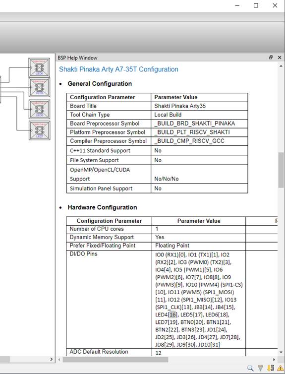
In the above code the USE_HAL_API pre-processor definition is used to enable HAL API code inside the Prerun and Run functions. CASP HAL APis for Shakti are declared in /hardware/swadeshi/shakti/shakti.h file. As you might have already noticed, CASP HAL APIs resembles Arduino Core APIs. This allows users to use them without learning a new API. The CASP HAL APIs used in the above code are pinMode, digitalRead and digitalWrite. pinMode is used to set direction (input or output) of a GPIO pin and digitalRead and digitalWrite are used to read from a and write to a GPIO pin respectively. Please note that the pin numbers mentioned are internal pin IDs used in CASP software for accessing hardware pins. Refer CASP BSP documentation for getting the internal pin ID for each GPIO pin. Sample screen shot of Shakti BSP documentation is given below. The internal pin ID is indicated in square braces of each pin label.
After the coding is done you may modify the model as shown below.
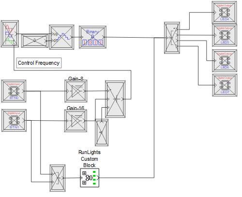
Since access to two BTN0, BTN1 and four LEDs are done inside the block code, the input output blocks of buttons and LEDs are no more required. As such they are disabled and only custom block is now enabled in the entire model. Set the custom block parameters are shown below

With the same simulation settings of Method-2, press Build/Run button. If errors are present in custom block source code it will be displayed in the Build window. If no errors are present the model will be build and the generated hex file will be uploaded to the FPGA board. The result should be same as that of Method-2.