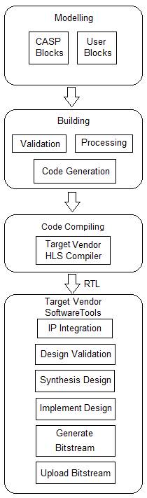
FPGA Workflow
CASP supports FPGA targets that support High Level Synthesis (HLS) compilers to convert untimed C/C++ code to Register Transfer Level (RTL). The FPGA development workflow in CASP consists of two basic steps:
· Generating RTL from CASP Model: CASP uses target HLS compiler to generate RTL from the user created model. This step follows workflow mentioned in previous topic.
· Generating Bit Stream File: In this step user has to use FPGA software design tools provided by the target vendor. The workflow largely depends on these software tools. However, typical FPGA design workflow consists of
o Integrating the RTL that is generated in the previous step with other RTL blocks. Typically, GUI based IP integrators are available from most of the FPGA vendors. CASP also provides some IPs that user can use during this step. User need not touch the hardware definition language (Verilog and VHDL) code if the complete logic is implemented in HLS.
o Design Validation
o Synthesis the design
o Implementation (place and route design) and optimization.
o Generating the final bit stream file.
Typical CASP FPGA Workflow